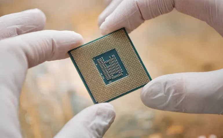
For more than half a century, the microelectronics industry has relied on Moore’s law—the observation that the number of transistors on an integrated circuit roughly doubles every two years—to drive performance gains. As traditional two-dimensional scaling approaches physical limits, engineers are turning to the third dimension. A recently announced prototype chip illustrates this shift by stacking 41 alternating layers of semiconductor and insulating material in a single device, opening a new pathway for continued progress.
Why Moore’s Law Is Stalling
Making transistors smaller has historically improved speed, reduced power consumption, and lowered cost. However, shrinking features below a few nanometres invites quantum tunnelling, excessive heat, and intolerable variability. Lithography equipment has also become prohibitively expensive, eroding the economic benefit that once accompanied each new “node.”
The 3-D Solution: Growing Up Instead of Out
The record-setting chip abandons strict planar design in favour of vertical integration. Much like high-rise buildings maximise limited city land, stacking circuitry upward multiplies transistor density without shrinking individual devices. Key elements include:
- 41 vertical tiers of silicon and dielectric material precisely deposited and patterned.
- Through-silicon vias (TSVs) that pierce the layers, providing ultra-short interconnects and reducing signal delay.
- Advanced thermal pathways to dissipate the additional heat generated in the stack.
Manufacturing Breakthroughs
Building a skyscraper inside a chip fab is non-trivial. Engineers relied on:
Atomic Layer Deposition (ALD): This technique grows films one atomic layer at a time, ensuring uniform thickness across tall structures.
Sequential Lithography: Multiple patterning steps align each new floor with nanometre precision.
Wafer Bonding: Separate wafers, pre-processed with circuitry, are bonded face-to-face to double the layer count in a single step.
Performance & Power Advantages
Because vertical distances are shorter than lateral ones, signals travel faster and consume less energy. Early measurements show:
- ~30 % lower interconnect delay compared with equally dense 2-D layouts.
- Up to 50 % reduction in interconnect power, a critical metric for battery-powered devices and data-centre efficiency.
- Higher overall transistor density without the leakage current penalties of further planar scaling.
Potential Applications
The technology is especially attractive for workloads that demand high bandwidth and low latency:
- AI accelerators that need large on-chip memory alongside compute cores.
- Edge devices where space is limited but performance cannot be sacrificed.
- 3-D NAND and DRAM extensions, blending logic and memory in a single package.
Remaining Challenges
Despite its promise, vertical scaling brings new obstacles:
- Thermal management: Heat tends to accumulate in interior layers, requiring innovative heat-spreading materials and micro-fluidic cooling.
- Yield: A defect in any layer can render the entire stack unusable, so process control must improve.
- Design tools: EDA software optimised for 2-D layouts must evolve to handle complex 3-D routing and timing analysis.
What It Means for the Future
The 41-layer demonstration chip is not merely a laboratory curiosity; it is a proof-of-concept that signals a paradigm shift. Instead of racing to the bottom of feature sizes, the semiconductor industry can unlock new performance gains by adding altitude. While Moore’s law in its original form may be fading, the spirit of relentless improvement lives on—now in three dimensions.
Key Takeaway
The next chapter of chip innovation will be written vertically. By embracing stacked architectures, engineers can continue to scale computing power in an era when traditional miniaturisation is running out of room.


